| Child pages (Children Display) | ||
|---|---|---|
|
| Table of Content Zone | ||||||||
|---|---|---|---|---|---|---|---|---|
| ||||||||
|
Overview
Sample cleanliness is extremely important for achieving good results in nanofabrication (hence the need for a cleanroom). However, simply working in the cleanroom does not guarantee cleanliness, proper steps need to be taken at every processing step to ensure a clean result. While some processes have more stringent cleanliness needs than others, some general rules apply for all types of lithography:
- Handle substrates/wafers with cleaned tweezers, not hands.
- Substrates should not be left exposed. Although the cleanroom offers nearly particle free air, particles are generated by the movement, plastic wafer carrier, talking, etc. Even in the cleanest areas of the cleanroom, particles will eventually find their way onto exposed surfaces.
Solvent Cleaning
Standard Process: TAI clean
- 5 min sonication in beaker of Toluene.
- 5 min sonication in beaker of Acetone.
- 5 min sonication in beaker of Isopropanol.
Background
Standard solvent cleaning is a three step process of ultrasonically agitating the substrate in subsequent solvent solutions to remove organic contamination. Three steps allow for selecting solvents that properly dissolve multiple types of contaminants. The first step is a nonpolar solvent (toluene) to remove any oils or grease present on the sample. The second step is a powerful polar solvent (acetone) to remove polar contaminants such as photoresist. The final step is a polar protic solvent (isopropanol).
Nonpolar Solvent Clean: Toluene
Toluene acts a nonpolar solvent to dissolve any grease or oil on the substrate. Nonpolar contaminants (especially fingerprints) will not be effectively removed by Acetone or IPA. (Interesting Fact: Toluene is used in the process to remove cocaine from coca leaves in the production of Coca-Cola syrup!!)
Polar Aprotic Solvent Clean: Acetone
Acetone's high dipole moment leads to a powerful cleaning of polar residue (such as photoresist). However its quick evaporation leads to residue redepositing on the substrate if evaporation is allowed to occur.
Polar Protic Solvent Clean: Isopropanol
IPA is used to remove fully wash away acetone from the substrate, and remove any remaining dissolved residue. As a result, IPA is mainly used to removing the Acetone without residue. However, unlike Acetone, IPA will form hydrogen bonds, and thus may provide some additional cleaning effects.
IPA is prefered as a final step over methanol. Its significantly slower evaporation rate results in less residue and a more forgiving rinse step. The close dipole moments of the two chemicals (DIPA=1.66 vs. DMethanol=1.69) means the difference between the two in cleaning ability is small, although methanol is somewhat stronger. From a safety standpoint, unlike Methanol, IPA is not considered toxic. And importantly for cleaning, "IPA is generally the purest available organic solvent and is used extensively for vapor drying of H2O-rinsed wafers." (Reinhardt 2008, p. 22)
If the clean is done immediately before spinning photoresist, a thorough IPA clean and dry should dehydrate the wafer, removing the need for a dehydration bake. If there is a significant delay between cleaning and spinning, ambient water will be adsorbed on the wafer surface. A dehydration bake should then be done.
Deionized Water Rinse
| Note |
|---|
A final DI rinse is usually optional, but is required for samples to be placed in furnaces. |
A powerful final step may be a rinse in the nanopure deionized water, which will assist in the removal of any remaining particles, solvent residues, and acid/base residues. However, if this step is employed before spinning photoresist, a dehydration bake must be performed to properly remove bound surface water molecules. This step is required for samples to be placed in any high temperature equipment or furnaces, as even slight solvent residue will combust at temperatures above 400 C.
Characterizing Cleanliness
Particle inspection (Particle size ~0.5 um and larger)
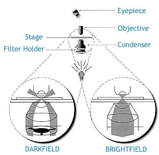
Inspection for contamination by particles 0.5 um or larger can be achieved readily through dark field microscopy.
In bright field illumination, the object is lit from below the stage, resulting in a larger, contrasted image that can be studied.
A dark field microscope is ideal for viewing objects that are unstained, transparent and absorb little or no light. These specimens often have similar refractive indices as their surroundings, making them hard to distinguish with other illumination techniques. A dark field microscope blocks this central light with a condenser so that only oblique rays hit the object. If there is nothing on the stage, the aperture of the condenser is greater than the objective and the view will be completely black. It is more useful in examining external details, such as outlines, edges, grain boundaries and surface defects than internal structure.
https://www.microscopeworld.com/t-darkfield_microscopy.aspx
Dark-field microscope (a) and top-view scanning electron microscope (SEM) (b) images of the same area on a silicon wafer ablated by a femtosecond laser. Microscope image is inverted in horizontal direction relative to that of the SEM. Selected nanoparticles are marked by corresponding numbers 1 to 6 in both figures.
Residual Metal Characterization
Metals present on a wafer can be quantitively characterized though a number of techniques, though we do not (to our knowledge) readily have the capabilities at Purdue to perform these measurements. Outside companies can be enlisted to perform ICP-MS / VPD ICP-MS to characterize what metals may be present on a sample. This is more cost effective than technologies such as TXRF, which show where on the wafer the contamination is rather than simply how much metal is present across the entire wafer.
Questions & Troubleshooting
Process Library
References
Presentations and Technical Sheets:
Solvents: Theory and Application (via Microchem)
Substrate Cleaning and Adhesion Promotion (Microchem)
Cleanliness, Contamination, and Chemical Handling (via SNF)
Textbooks:
Handbook of Silicon Wafer Cleaning Technology, Karen A. Reinhardt and Werner Kern, 2008.
Handbook of Semiconductor Manufacturing Technology, Robert Doering and Yoshio Nishi, 2007.
Piranha:
University of Cambridge Piranha guidelines (dead link)
RCA Standard Clean:

