- Created by Neil Dilley on Oct 16, 2023
You are viewing an old version of this page. View the current version.
Compare with Current View Page History
Version 1 Next »
Terminology
Wet Etching - Substrates are immersed in a reactive solution (etchant). The layer to be etched is removed by chemical reaction or by dissolution. The reaction products must be soluble and are carried away by the etchant solution. Generally, wet etching is isotropic.
Dry Etching - Substrates are immersed in a reactive gas (plasma). The layer to be etched is removed by chemical reactions and/or physical means (ion bombardment). The reaction products must be volatile and are carried away in the gas stream.
- Plasma Etching - Typically high pressure, no ion bombardment. (Substrate is placed on a grounded electrode)
- Reactive Ion Etching - Typically lower pressures, ion bombardment. (Substrate is placed on a powered electrode)
Anisotropic Etch - Etch rate is not equal in all directions.
Isotropic Etch - Etch rate is equal in all directions.
Etching - The process by which material is removed from a surface.
Mask - Used to protect regions of the wafer surface. Examples include photoresist, Ni, Cr, or oxide layer.
Selectivity - The ratio of etch rate of film to etch rate of substrate or mask.
Aspect Ratio - Ratio of depth to width of an etched feature.
Plasma - Partially ionized gas containing an equal number of positive and negative charges, as well as some other number of none ionized gas particles.
Glow Discharge - Globally neutral, but contains regions of net positive and negative charge. (Many thin film processes utilize glow discharges, but “plasma” and “glow discharge” are often used interchangeably)
Plasma Fundamentals
The fourth state of matter, an ionized gas into which sufficient energy is provided to free electrons from atoms or molecules and to allow neutral molecules, radicals, ions and electrons to coexist. Below is a high level overview of plasma fundamental physics. For a more details look at plasma, see the paper "A Short Introduction to Plasma Physics".
Typical Plasma Composition | |
Neutral Molecules
|
|
Radicals
|
|
Electrons
|
|
Positive and Negative Ions
|
|
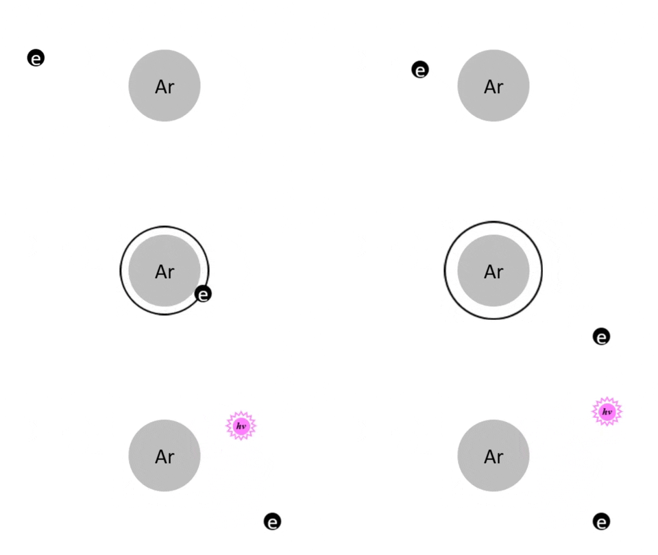
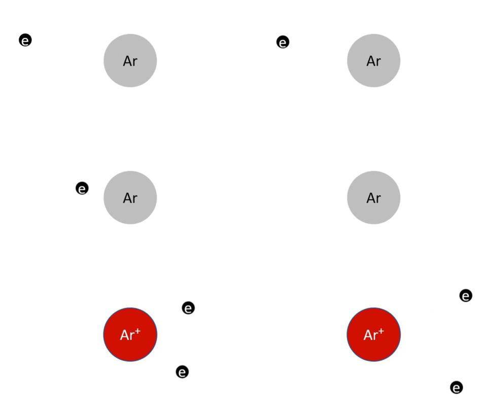
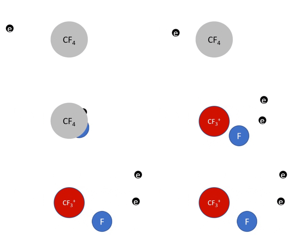
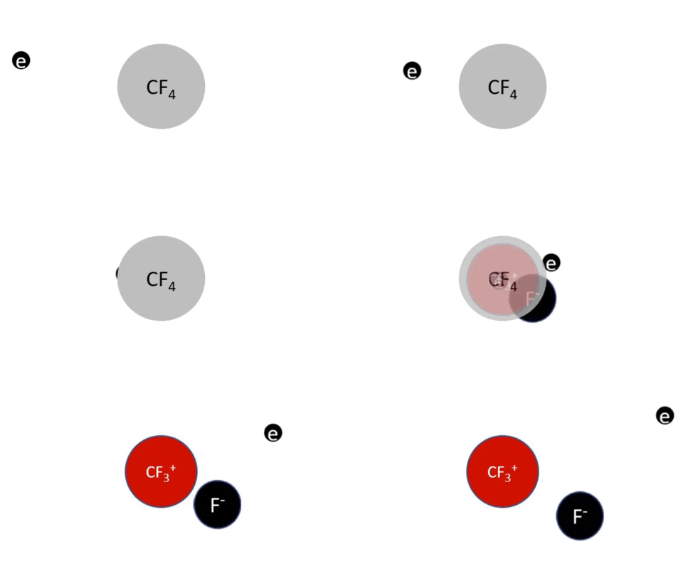
Collision Processes and the Production of Active Species | |
|---|---|
Electron Excitation
|
|
Simple Ionization
|
|
Dissociative Ionization
 |
|
Dissociative Ionization with Attachment
|
|
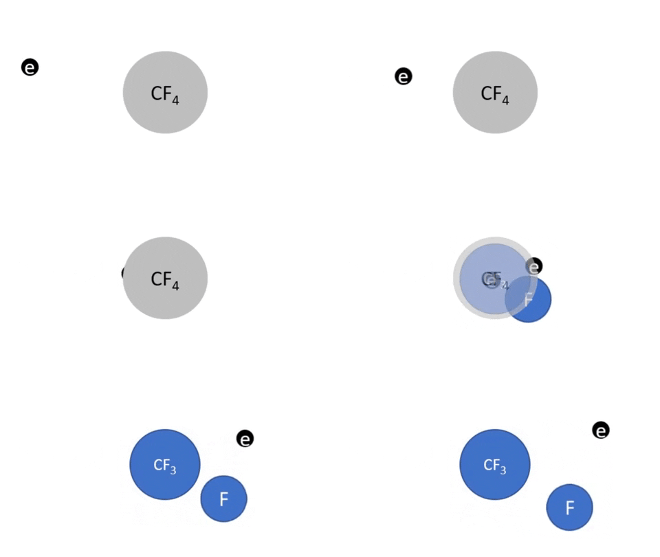
Molecular Dissociation, Radical Formation
|
|
Plasma Loss MechanismsIn a stable plasma, unstable particles are continuously generated and lost. The concentration of ions, radicals, and electrons increase until their loss rate is equal to their generation rate and steady state is reached. | |
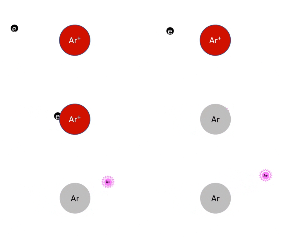
Recombination of Ions and Electrons
|
|
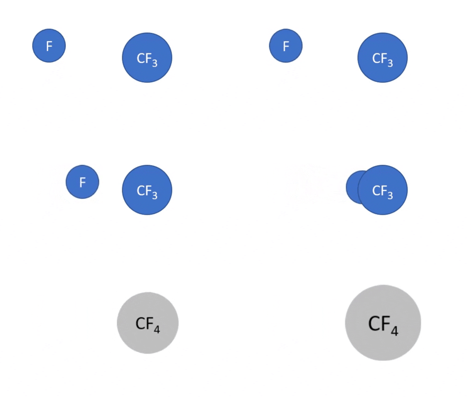
Recombination of Radicals
|
|
Chemical Reaction
|
|
Drift and Diffusion
|
|
How is Plasma Made | |
DC Glow Discharge
| .gif?version=1&modificationDate=1697503603000&cacheVersion=1&api=v2&width=400&height=224) |
RF Plasma
|
|
Dry Etch Fundamentals
Dry Etch Material Removal Mechanisms | |
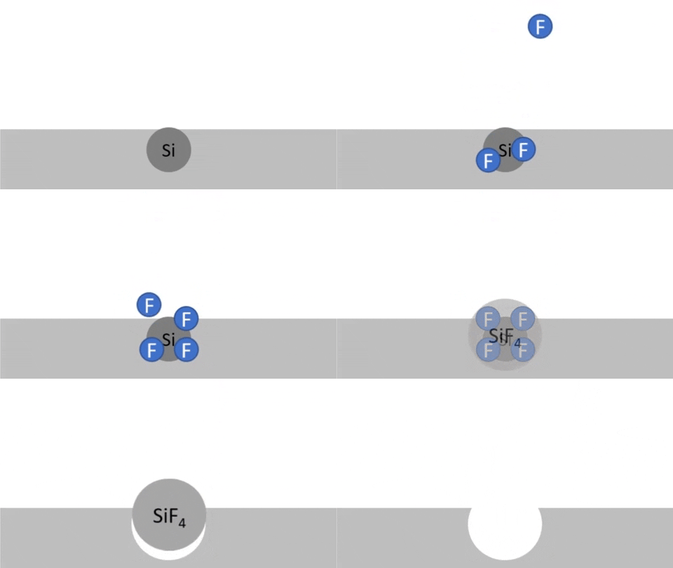
Reactive Etching
|
|
Ion Etching
|
|
Reactive Ion Etching
|
|
Dry Etching Equipment Configurations | |
Capacitive RIE Etch Chamber
|
|
Inductive RIE Etch Chamber
|
|
Directionality of Etching | |
Degree of Anisotropy (A)
|
|
Vertical Etch
|
|
Anisotropic Etch
|
|
Isotropic Etch
|
|
Compatibility of Fluorine and Chlorine Etch Chemistry in a Shared Etch Tool
Reactive ion etch processing is known to exhibit significant variability in final etch performance due to wall condition. Previous studies have shown that neutral species transients depend strongly upon chamber seasoning.
| Effects of Cl2 and Fluorine Chemistry on Chamber Walls and Etch Parameters | |||||||||||||||||||||||||||||
New chamber walls conditioning and cleaning strategies to improve the stability of plasma processes Changes in the chamber wall conditions (e.g. chemical composition) are identified as being one important cause of process drifts such as changes in etch rates, etching profiles, etching selectivity or etching uniformity across the wafer. As the reactor wall conditions are modified due to the deposition or removal of etch products, the plasma chemistry changes, which in turn modifies the process performances. Controlling the reactor wall conditions and their stability is of primary concern when trying to create repeatable processes. In the plot to the right, the first column (a) represents a new, unaltered, Al2O3 chamber wall. In the second column (b), we see the effect of Chlorine etching. There is a clear build up of Silicon Oxychloride layers, as well as, Cl+Br bonded to the wall. The third column (c) represents an 80s fluorine etch following the chlorine etch. We see that the Silicon Oxychloride film and Cl+Br bonds have been removed and we are left with a thin fluorinated aluminum layer. Column (d) represents subsequent fluorine etches totaling 20 minutes of plasma exposure. We see that the fluorinated aluminum layer is building but surface chemistry has not changed. This will lead to several issues including flake off of AlxFy particles on the wafer and process drifts (due both to the progressive growth of AlF material on the SiO2 windows and to the release of F atoms from the chamber walls during the etching process). Plasma chemistry can be used to control the conditioning of the chamber. Transitions from chlorine to fluorine and visa versa require different approaches, see below for details. |
| ||||||||||||||||||||||||||||
| Transition from Fluorine to Chlorine etch chemistry | |||||||||||||||||||||||||||||
|---|---|---|---|---|---|---|---|---|---|---|---|---|---|---|---|---|---|---|---|---|---|---|---|---|---|---|---|---|---|
Observed Effects A thin film of silicon oxychloride grows on the chamber walls during Chlorine plasma etches. Fluorine etch chemistry will quickly strip away the thin oxychloride film from chamber walls resulting in significant transient effects in plasma density and real-time etch rate when transitioning back to chlorine etch chemistry. The root cause of these transients is assumed to be a result of dynamic oxychloride layer build-up processes at the chamber walls. As shown in the plot to the right, Chlorine etch rate will be lower when transitioning from Fluorine etch back to Chlorine etching. Chlorine etch rate will also be lower when following a chamber mechanical clean as this can also strip the oxychloride film from the chamber walls. |
Black trace represents a well seasoned chamber. Green trace represents first Chlorine etch after Fluorine etch. | ||||||||||||||||||||||||||||
Proposed Mechanism for Effects The transient effects of oxychloride film buildup persist until it has achieved a steady state creation/loss ratio. At this point the Chlorine etch conditions become constant. In the paper referenced, it is suggested that transient effects are eliminated after approximately 300 seconds of Chlorine etching. The chamber seasoning alters recombination rates at the walls, which affects both the neutral species density and the plasma density as shown in the plot to the right. The plot shows that SiCl4 is low and increasing at the start of first Chlorine etch after a Fluorine etching. SiCl4 is the primary etch product of Si etched in Cl2 chemistry and is a good indicator of real time etch rate. |
Black trace represents a well seasoned chamber. Green trace represents first Chlorine etch after Fluorine etch. | ||||||||||||||||||||||||||||
Recommended Chlorine Etch Chamber Preparation In our shared facility, it is often difficult to know exactly what has happened in the chamber before you arrived to use the tool. In addition, most users are more concerned with final depth of their etch rather than efficiency of time usage. For these reasons, it is best to return the chamber to a known condition before you begin your processing. Since the transient effects discussed above are consistent and predictable, we can generate a recipe that will bring the chamber to a stable condition before Chlorine etching. Before beginning your Chlorine etch, it is best to strip the oxychloride film from the chamber walls and bring the chamber walls back to a known starting point. Do this by running the clean and coat recipe available at the tool. Once returned to the known starting point, you may proceed with your Chlorine etch as usual. Example Recipe for Panasonic E620 (other tool recipes may vary from this but purpose is the same)
|
Chlorine etch depth achieved for first three etches after Fluorine etching. Samples etched for 30 seconds each, significant etch rate increase for each sample. This is known as the "First Wafer Effect" in industry. The etch rate is increasing for each run as the wall seasons with | ||||||||||||||||||||||||||||
| Transition from Chlorine to Fluorine etch chemistry | |||||||||||||||||||||||||||||
Observed Effects During Chlorine plasma etches a thin film of silicon oxychloride grows on the chamber walls. Fluorine etch chemistry will strip away the thin oxychloride film from chamber walls resulting in significant transient effects in plasma density and real-time etch rate when transitioning back to fluorine etch chemistry. The root cause of these transients is assumed to be a result of dynamic oxychloride layer stripping processes at the chamber walls and subsequent build up of Al-F layers. The oxychloride stripping effects of fluorine etch plasma are short lived and typically last less than a minute. The subsequent build up of Al-F layers can take a few minutes to stabilize. |
Black trace represents a Cl2 seasoned chamber. Green trace represents first Chlorine etch after Fluorine etching, indicating plasma losses due to replacing oxychloride film that was stripped in a 30 second fluorine etch. | ||||||||||||||||||||||||||||
Proposed Mechanism for Effects The transient effects of oxychloride film stripping persist until the film has been removed. At this point the fluorine etch conditions become constant. In the paper referenced, it is suggested that transient effects are eliminated after approximately 30 seconds of fluorine etching. The chamber seasoning alters recombination rates at the walls, which affects both the neutral species density and the plasma density as shown in the plot to the right. The plot shows that SiCl4 is low and increasing at the start of first Chlorine etch after a Fluorine etching. SiCl4 is the primary etch product of Si etched in Cl2 chemistry and indicates low etch rate due to plasma losses. |
Black trace represents a Cl2 seasoned chamber. Green trace represents first Chlorine etch after Fluorine etching, indicating low etch product due to replacing oxychloride film that was stripped in a 30 second fluorine etch. | ||||||||||||||||||||||||||||
| Recommended Fluorine Etch Chamber Preparation In our shared facility, it is often difficult to know exactly what has happened in the chamber before you arrived to use the tool. In addition, most users are more concerned with final depth of their etch rather than efficiency of time usage. For these reasons, it is best to return the chamber to a known condition before you begin your processing. Since the transient effects discussed above are consistent and predictable, we can generate a recipe that will bring the chamber to a stable condition before fluorine etching. Before beginning your fluorine etch, it is best to strip the oxychloride film from the chamber walls and bring the chamber walls back to a known starting point. Do this by running the chamber clean recipe available at the tool. Once returned to the known starting point, you may proceed with your fluorine etch as usual. Example Recipe for Panasonic E620 (other tool recipes may vary from this but purpose is the same)
|
Chlorine etch depth achieved for first three etches after Fluorine etching. The etch rate is increasing for each run as the wall seasons with oxychloride buildup and the recombination rate goes down, indicating previous fluorine etch stripped oxychloride film. | ||||||||||||||||||||||||||||
References
Introduction to Plasma Etching_Lecture_102417_Day2_sntzd.pdf
BookDry etch for semiconductors _Nojiri.pdf
Oxford Plama Etching Media Center
Materials
Aluminum Oxide
From a quick search, seems to be typically etched in high density plasmas with a chlorine based chemistry - JCW
The ETCH Mechanism for Al2O3 in Fluorine and Chlorine Based RF Dry Etch Plasmas
Temperature dependence on dry etching of Al2O3 thin films in BCl3/Cl2/Ar plasma
Dry Etching of Al2O3 Thin Films in O2/BCl3/Ar Inductively Coupled Plasma
General - Will it etch
Materials can generally be etched in the RIEs as long as they form volatile byproducts, or products for which the vapor pressure (at the temperature of the etch) is higher than the pressure of the chamber.
Etching is very complicated and this will be massive oversimplification...but generally volatile byproducts can be determined from literature, or as a fallback, the CRC Handbook of Chemistry and Physics Online, (4) Properties of the Elements & Inorganics, Physical Constants of Inorganic Compounds: https://hbcp.chemnetbase.com/faces/documents/04_02/04_02_0001.xhtml. From there, click "Go to Interactive Table", and find products that may be formed (i.e. chloride, fluorides, oxides, depending on the gasses). A compound is deemed volatile if it has a boiling point at a reasonable temperature range for the temperature and pressure of the system. Note that at lower pressures, boiling points decrease, so these are just a good staring point reference.
As a VERY general rule of thumb, anything with a boiling point (tbp) < 185 C will be volatile in the ICP RIEs.
As an example, aluminum chloride is volatile, and aluminum fluoride and aluminum are not.
![]()
![]()
![]()
![]()
Neither Copper chloride or copper fluoride is volatile, which is why it is not allowed in any chamber:
![]()
![]()
![]()
![]()
![]()
![]()
Byproducts of silicon are very volatile:
![]()
![]()
Many times different fluorides/chlorides of the same material will have drastically different boiling points. It's important to research which will be formed in the plasma. Titanium is a good example of this, with TiCl2 and TiCl3 being non-volatile, and TiCl4 being volatile:
![]()
![]()
![]()
Mounting
Small samples may be mounted to carrier wafers with Crystalbond 555 HMP. More info here: A09_18.pdf and 821-1-2-3-4-6-TN.pdf
Basic Procedure: Attaching a Sample to a Carrier Wafer Using Crystalbond.pdf
Detailed Paper on Attaching Samples from Stanford: https://snfexfab.stanford.edu/docs/process/attaching-samples-to-carrier-wafers-for-etching-or-deposition
- No labels


