Surface Characterization
- Former user (Deleted)
- Neil Dilley
- Wirth, Justin C
- Hosler, Richard S
Owned by Former user (Deleted)
Last updated: Nov 01, 2024 by Neil Dilley
Overview
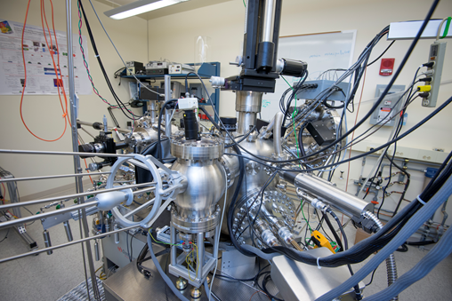
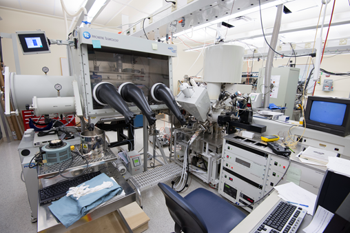
Omicron surface analysis cluster
- X-ray photoelectron spectroscopy (XPS) -- surface chemical composition
- low energy electron diffraction (LEED) – macroscopic surface structure
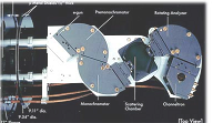
- state-of-the-art UHV scanning tunneling microscopy and atomic force microscopy (STM/AFM) – atomic arrangement
- high-resolution electron energy loss spectroscopy (HREELS) -- vibrational structure (adsorbed species, phonons, etc.)
- synthesize a material with required surface composition under UHV and to perform full characterization without taking the sample out
- UHV treatment chamber (120 K – 1000 K), various gasses including metal-organic precursors, mass-spectrometer, also following deposition capabilities:
- e-beam evaporators (2 sources for simultaneous use)
- thermal evaporators (Zn, Te, Bi, Se; other metals possible)
- sputtering source for refractory metals (Ta, etc.)
- gas manifolds for UHV atomic layer deposition (ALD)
- atomic hydrogen source, etc.
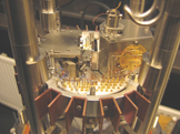
Kratos Axis Ultra DLD imaging XPS instrument
- Monochromatic X-ray source to minimize radioactive and thermal damage and improve the resolution
- Charge neutralizer to study non-conducting samples minimizing non-homogeneous charge and improving the resolution
- Real time imaging XPS to allow x- y- chemical mapping
- Reaction cell (CatCell) to treat samples under different gas mixtures up to 6 bar at up to 1000°C, the transfer between the CatCell and the analysis chamber is under UHV without any contact to air
- Sputtering gun, which can use either Ar+ or coronene (C24) for non-destructive depth profiling
- UV-lamp to perform Ultra-Violet Photoemission Spectroscopy (UPS)
- Ar-filled glove-box attached directly to the entry-lock of the XPS instrument to analyze air- and moisture sensitive samples (for instance Li ion battery or transition metal dichalcogenides, etc.)
Senior Research Scientist in charge: Dmitry Zemlyanov
Panalytical MRD X'Pert Pro high resolution x-ray diffractometer (XRD)
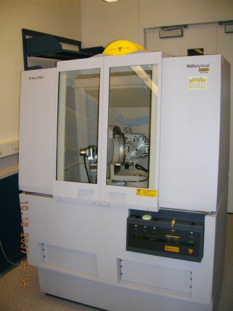
- thin films, both single crystal and polycrystalline (diffraction & XRR), size up to 4” wafer
- Anton Paar DHS 900 domed hot stage for measurements up to 900°C
- Crystal orientation/offcut
- Degree of crystallinity
- Stresses/strain of single crystal thin film
- Spatial mapping (100 x 100 mm motion) of sample surfaces
- High speed wide angle x-ray diffraction and fast mode reciprocal space mapping
- Density and film thickness determination (x-ray reflectivity XRR)
- Pole figure
- Low angle measurement as low as 0.1 °
Research Scientist in charge: Hakan Salihoglu
- Kratos X-ray Photoelectron Spectrometer
- Omicron Surface Analysis Cluster
- Panalytical X'pert Pro (XRD)
- Glovebox - BRK 1077
- Glovebox - Kratos Axis Ultra DLD XPS
, multiple selections available,