/
Patterning
Patterning
- Wirth, Justin C
- Neil Dilley
- Former user (Deleted)
Owned by Wirth, Justin C
Last updated: Apr 03, 2024 by Neil Dilley
Overview
Optical Lithography
- Heidelberg MLA150 Maskless Aligner: for mask-making or direct write photolithography
- Suss MA6 Mask Aligner
- Suss MJB3 UV400 Mask Aligner
- Suss MJB4 UV400 Mask Aligner
Electron Beam Lithography
JEOL JBX-8100FS
- 100kV max beam energy
- 125 MHz scan speed
- Resolutions down to 7nm
- 2 Modes:
- High Throughput - 1000um Field Size
- High Resolution - 100um Field Size
- Cassettes for pieces: 3”, 4”, 6” wafers, 5” photomasks
- GenISys Beamer software
Raith: e LiNE
- 30kV max beam energy
- 20 MHz scan speed
- Resolutions down to 18nm
- Standard or Ultra-flat Cassette
- Up to 4” wafer
- Excellent SEM imaging
- Excellent for work on nanowires, graphene, carbon nanotubes
Other patterning
- Nanonex NX-2000: nano-imprint lithography tool for making multiple copies of small geometry patterns
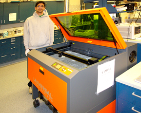
- PLS6MW Laser Engraver
- Photoresist Dry Film Laminator
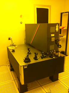
- Interference Lithography System
- Laurell EDC-650 Spin Processor
Staff contact: Ron Reger
- Photomask Fabrication
- Spin Coating
- Photoresist Baking
- Optical Lithography
- Electron Beam Lithography
- Other Patterning
- Test patterns
Any patterning begins with a pattern, usually in GDS or OAS. See this youtube tutorial on KLayout: https://www.youtube.com/channel/UC45cUNKyJLlRDqCsL1QZFPQ/videos
, multiple selections available,
Related content
Processing
Processing
More like this
Fabrication
Fabrication
More like this
Optical Lithography
Optical Lithography
More like this
Cleaning
Cleaning
Read with this
Photomask Fabrication
Photomask Fabrication
More like this
ASAP-1 IPS Digital Sample Preparation System
ASAP-1 IPS Digital Sample Preparation System
Read with this